Electromigration (EM) is a phenomenon where metal ions in an interconnect get displaced due to the flow of electrons. You need to consider how this affects our circuit designs, especially with the increase in current densities over time. When too much current flows through a small metal wire, the metal atoms can shift, causing voids (gaps) or hillocks (bumps) that eventually lead to failure.
What Causes Electromigration (EM)?
Electromigration happens when there’s excessive current density (J), which is determined by the formula:
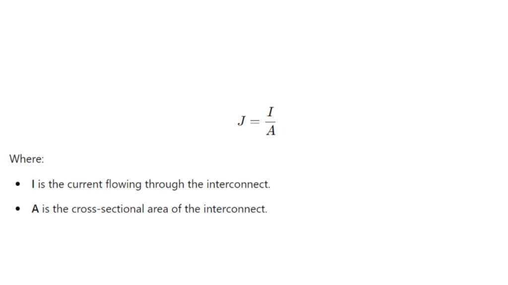
When you have higher currents (I) or thinner wires (A), electromigration becomes a bigger issue. So, as we shrink the size of interconnects in modern chips, the risk of EM increases.
What is Parasitic Channel Formation in MOSFETs: Causes and Solutions
How Can You Prevent Electromigration?
Although we can’t completely stop electromigration, there are several methods you and I can use to reduce its effects:
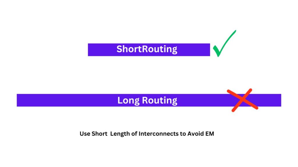
Use Short Length of Interconnects: If we keep the length of interconnects below a certain threshold (called the “Blech length“), electromigration won’t cause failures. Breaking long wires into shorter segments can help. This approach makes each segment more resistant to EM, but it can increase routing complexity.
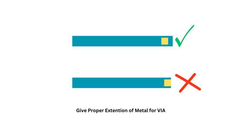
Give More Metal Enclosure: By providing extra metal at certain points (like enlarging via overlaps), we create a “reservoir” of material for the migrating metal atoms. This helps prevent voids that could break the interconnect. However, this may not always be effective when the direction of the current flow reverses.
Optimize Via Configurations: Vias, which connect different layers of metal, are key areas for EM. Placing vias “below” the metal line is better than placing them “above” because it allows for a higher tolerance of voids, making the interconnect more resistant to EM damage.
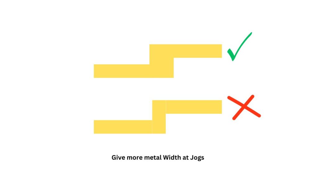
Avoid Metal Jogs: If possible, please avoid Metal Jogs, Because it will increase the possibility of EM, increase current density.
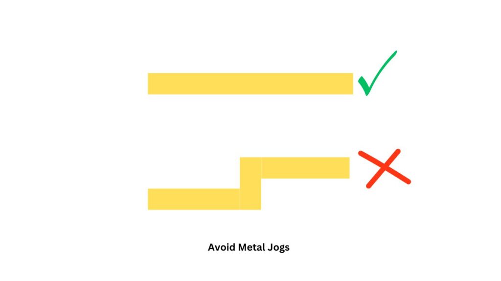
Give more metal Width at Jogs: If it is not possible to use strait metal, And if you want to use Jog, then give more width for jog area.
Use Via Arrays: When possible, we should use multiple vias in parallel. This ensures that the current is distributed evenly, reducing the current density in any one via and lowering the risk of EM.

Avoid Sharp Corners: In bends of interconnects, especially at 90-degree angles, current density can spike, increasing the risk of EM. Using smoother, more gradual bends (like 135 degrees) helps reduce this risk.

Optimize the Net Topology: By carefully designing the interconnect paths (net topology), we can split the current into multiple paths. This reduces the current density in any one path and spreads out the risk of EM.
Using Tools to Analyze EM
You can also rely on modern design tools that have features to analyze and prevent EM. These tools can optimize the wire sizes, balance current densities, and simulate how the stress builds up over time. For more complex designs, such as analog or power circuits, using detailed simulations (like finite element analysis) can give us a more accurate view of where EM might become a problem.
Conclusion
Electromigration is a serious concern in today’s smaller, more powerful chips. However, by using techniques like shorter interconnects, via arrays, and optimized routing paths, we can manage and mitigate the risks. The right tools and strategies can help ensure your designs remain reliable, even with the challenges that EM presents.