

 VLSI Master asked 2 years ago
 semiconductor answered 2 years ago
In my opinion, the fabrication process seems quite detailed. First, a SOI wafer is used as the starting material. Then, a stack layer of CVD Si N and SiO is deposited on the silicon film to create a hard mask. Electron beam lithography patterns the fine Si-fin.
 DigitalWorld answered 2 years ago
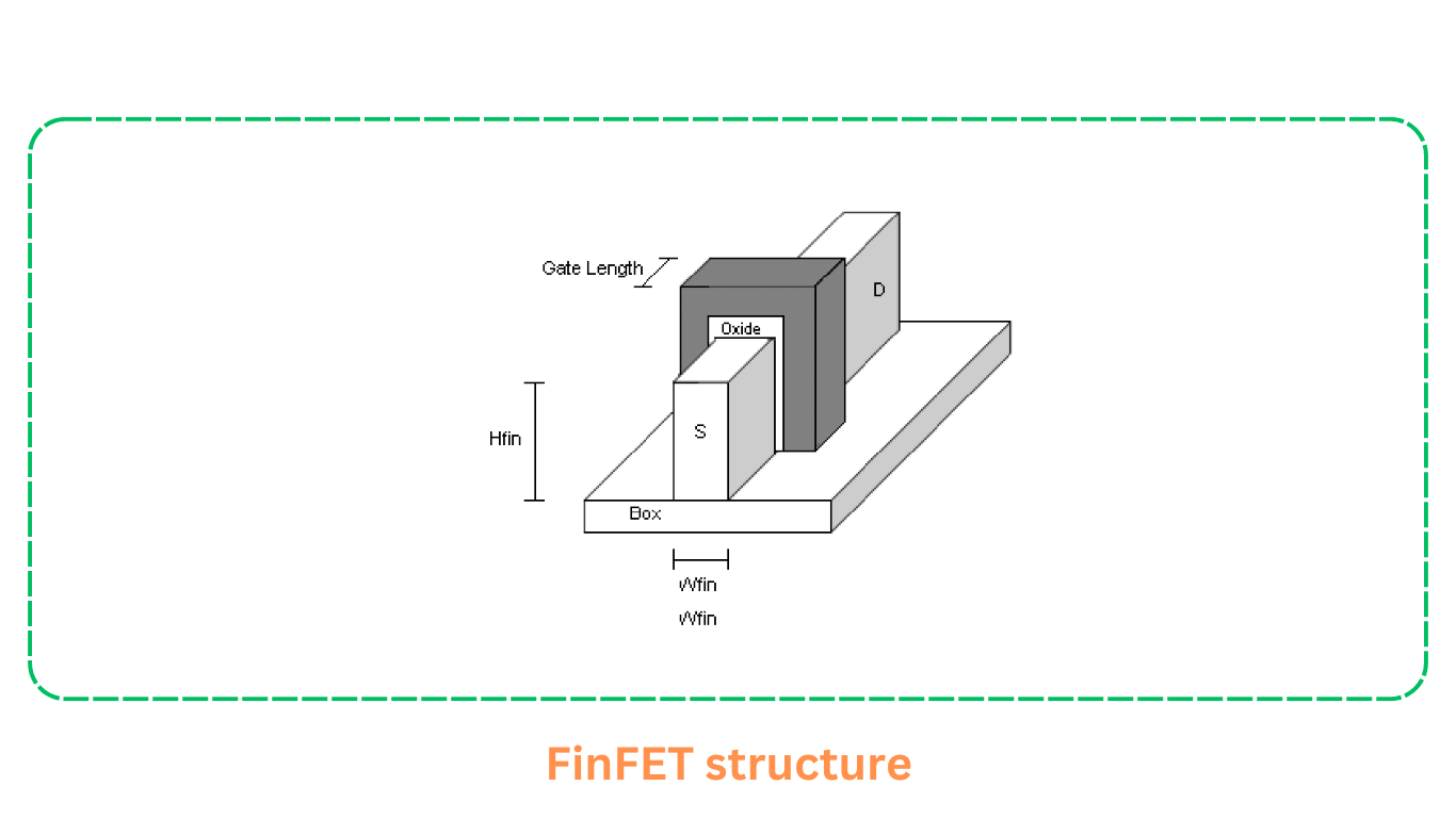
I've read about this too. The thin silicon fin is the core of the FinFET, acting as the body of the MOSFET. A heavily doped poly-Si film wraps around the fin, making electrical contact with its vertical faces. You know, this helps in reducing the source/drain series resistance.
 TechGuru answered 2 years ago
I agree with you. The process involves several steps, including etching the SOI layer to expose the silicon only on the sides of the fin. The in-situ phosphorus-doped amorphous silicon is then deposited to form the source/drain pads. You can see the attention to detail in these steps.
 CodeBook answered 2 years ago
For me, the interesting part is the use of different materials like SiGe for the gate, which improves compatibility with the poly-Si gate process. Also, the self-aligned double gates help in reducing parasitic capacitance and resistance. It’s fascinating how precise the measurements have to be, especially with such tiny dimensions.
Please login or Register to submit your answer