Analog Layout
Analog layout involves various critical elements such as Sharing, Fingering, Matching, Shielding, and crosstalk management. Sharing refers to the efficient use of layout resources among different circuit blocks. Fingering entails optimizing the routing paths to minimize parasitic effects. Matching ensures consistent performance of paired components.
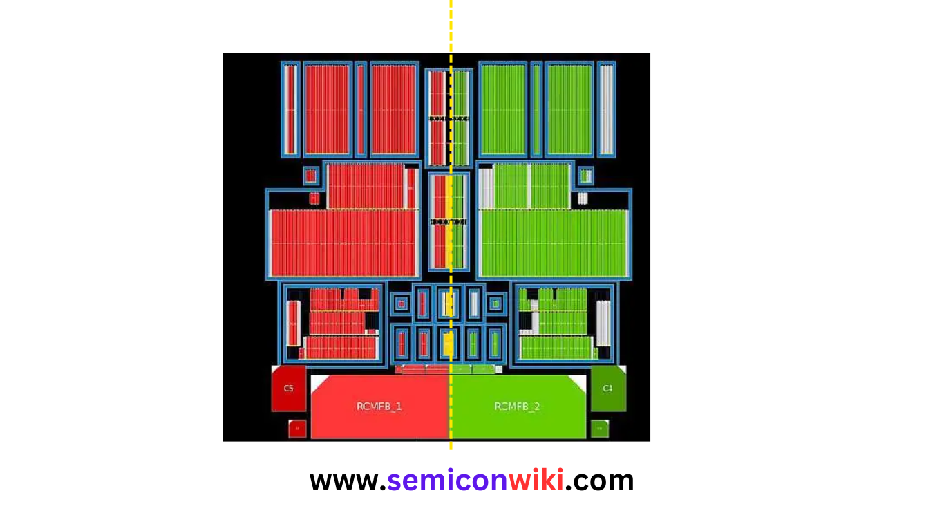
Analog Layout Example(Image source)
Shielding techniques are employed to mitigate interference and crosstalk between adjacent components. Additionally, understanding second-order and Short-channel channel effects is crucial for accurate analog design, as they affect transistor behavior and overall circuit performance.
Related: Top 10 Analog Layout Interview Questions(2024)
Important Points in Analog Layout
- Sharing: Components on the layout share common resources such as power or ground connections to optimize space and reduce routing complexity.
- Fingering: Involves arranging interconnects in a way that minimizes resistance, capacitance, and electromagnetic interference, enhancing circuit performance.
- Matching: Ensures that critical components, such as transistors or resistors, have identical characteristics to maintain balance and symmetry in the circuit, crucial for precision and stability.
- Shielding & Crosstalk: Utilizes physical barriers and isolation techniques to minimize interference between adjacent components, reducing signal distortion and improving signal integrity.
How Can You Become an Analog Layout Engineer?
If you’re aiming to become an Analog Layout Engineer, you’ll need to start by getting a Diploma in ECE or EEE, or even better, a bachelor’s degree in Electrical Engineering or a related field. From what I’ve seen, many companies are open to hiring candidates for entry-level positions if you’ve completed some hands-on layout design training—even if you’re just starting out.
As Analog Layout Engineers, we focus on designing and developing the circuitry inside many of the analog devices you and I use every day. Our job is to create, test, and fine-tune circuits to make sure they function properly and reliably.
We also don’t work alone. Often, we collaborate with the manufacturing team to ensure the design is built exactly as planned. The role can be demanding, and there are times when you might have to put in extra hours to meet tight deadlines—but it’s also a field where you really get to build something meaningful.
Related Posts
Memory Design Interview Questions
Physical Design Interview Questions
STA Interview Questions
Verilog Interview Questions