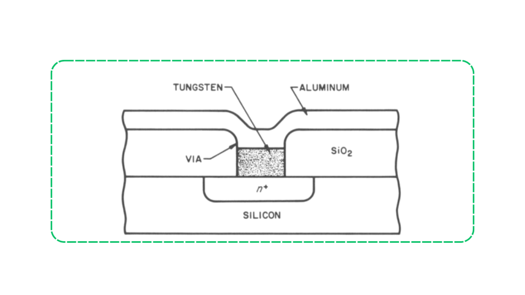
We fill via holes with tungsten in VLSI technology because tungsten has low stress and high resistance to electromigration, which makes it a reliable material for ensuring good electrical connections. I think you can see how important these properties are for maintaining the integrity of the connections in integrated circuits. Additionally, tungsten adheres well to materials like silicon, aluminium, and silicide’s, which helps in creating strong, self-aligned structures.(Image source)
Challenges associated with using tungsten for via hole filling
However, there are challenges associated with using tungsten for via hole filling. One major issue is that tungsten does not stick well to SiO2 unless there are nucleation sites available. To avoid unwanted tungsten growth on SiO2 surfaces, we need to ensure proper cleaning procedures. Another challenge is the potential for tungsten to laterally encroach under the oxide, which can cause loss of selectivity and form “worm holes” in silicon. This can lead to defects and reliability issues.
Aspect Ratio of Vias
Moreover, as the aspect ratio of the vias increases, shadowing effects during tungsten deposition can cause voids at the top edges of the vias. These voids can create weak spots in the connections. To mitigate this, reactive sputter etch can be used to open up the voids. Despite these challenges, the benefits of using tungsten, such as its resistance to electromigration and its compatibility with IC technologies, make it a valuable material for via hole filling in VLSI technology.
Advantages of Tungsten Metal
If you’re working with high-performance materials, you’ve probably come across Tungsten. It’s one of the toughest metals we use in engineering and electronics. Here’s why Tungsten stands out:
- Extremely High Melting Point: You and I can rely on Tungsten in applications that face intense heat. It has the highest melting point of all metals—over 3400°C.
- High Density and Strength: Tungsten is incredibly dense and strong, making it perfect for heavy-duty components, including aerospace and military uses.
- Excellent Electrical Conductivity: We often use Tungsten in electronic devices because it handles electricity well without deforming under heat.
- Corrosion Resistance: You don’t have to worry much about Tungsten rusting or corroding—it stays stable even in harsh environments.
- Durability: Whether it’s used in filaments, electrodes, or cutting tools, Tungsten lasts longer under stress compared to many other metals.