When it comes to N-PLUS (NMOS Source-Drain) or NSD and P-PLUS (PMOS Source-Drain) or PSD masks, you might wonder why these are necessary in the process of fabricating Field-Effect Transistors (FETs). Let me break it down for you in simpler terms.
Use of NSD and PSD mask in VLSI
First of all, when we’re creating the source and drain regions for NMOS and PMOS transistors, we use masks like N-PLUS and P-PLUS to help define the precise edges of these regions. Now, you might ask, why is it important to define these edges so carefully? Well, by using the N-PLUS and P-PLUS masks, we can control where the source and drain regions end in relation to the gate structure. This is important because it helps in minimizing unwanted effects like parasitic capacitances, which can negatively affect the performance of the transistor.
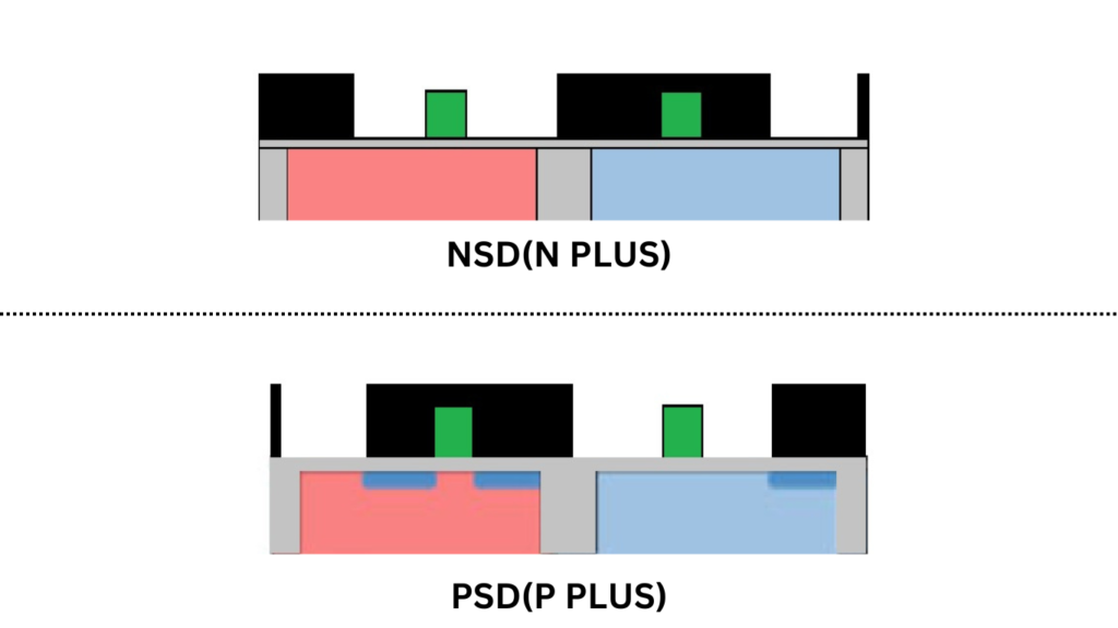
When you think about it, having precise control over these regions means we are reducing overlaps between the gate and the source or drain areas. This overlap is something we usually want to minimize because it can lead to unnecessary capacitance (like CGS and CGD, which stand for capacitances between gate-source and gate-drain). Lower capacitance helps the transistor switch faster, which is essential for faster and more efficient circuits.
We also use these N-PLUS and P-PLUS masks for doping the bulk contacts of the NMOS and PMOS transistors, respectively. In simpler terms, this means we are controlling how much and where the doping happens to ensure that the FETs work correctly in their respective wells—NMOS in n-well and PMOS in p-well.
So, when you’re considering why N-PLUS and P-PLUS masks are needed, remember that they are essential for precision, performance, and reliability in transistor fabrication. It’s all about making sure everything is aligned and functioning optimally.
P-Type Substrate in Semiconductor Design
If you’re diving into semiconductor design, one of the first things you’ll come across is the p-type substrate. When we use a p-type substrate, we’re working with a silicon wafer that’s doped with trivalent elements, like boron. This doping introduces holes (positive charge carriers), which become the majority carriers in the silicon crystal.
These holes help the material conduct electricity more efficiently and serve as the foundation for building active and passive devices on the chip. As you design circuits, the characteristics of this substrate—especially its doping profile—play a big role in how well you can manage device isolation, parasitic effects, and biasing strategies.
So, if you’re designing CMOS or any integrated device, understanding the behavior of the p-type substrate is essential to achieving good performance and reliable operation.