Cut Mask
In the SADP process, we use a cut mask, also known as a block mask, to trim the tips of lines created in the first litho-etch step or to remove dummy lines. You might wonder why this cut mask is necessary. The reason is that the initial step of creating lines often results in extensions that are not needed or dummy lines that can interfere with the design. By using the cut mask, we can precisely define the ends of the functional lines and remove any unnecessary parts. This step is crucial because it ensures that the final pattern is accurate and free of defects that could impact the performance of the semiconductor device.
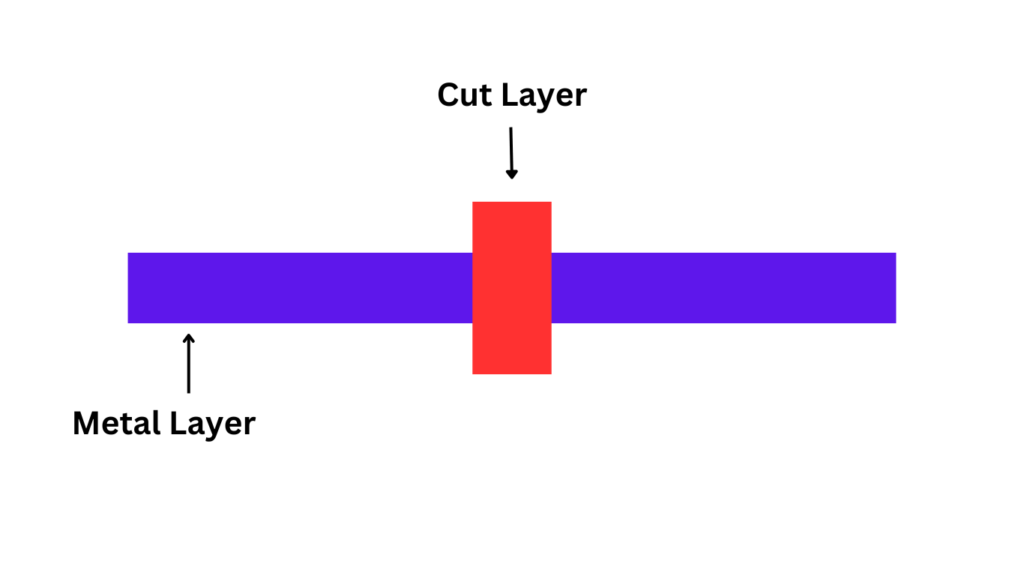
In summary, we use the cut mask in the SADP process to refine the line ends and eliminate unwanted elements, which helps in achieving a more reliable and precise manufacturing outcome. By understanding the role of the cut mask, you can appreciate how it contributes to minimizing variation and enhancing the overall quality of the semiconductor fabrication process.
Why SADP process is better than LELE?
SADP is an advanced method used in semiconductor manufacturing, distinct from the traditional litho-etch-litho-etch (LELE) process. While LELE uses two masks that need precise alignment, SADP relies on spacers that are self-aligned to the first litho-etch step, reducing the risk of misalignment.
Use of Cut Layers in VLSI?
In VLSI, we use CUT layers to address the challenges that arise from double patterning (DP) design rules, especially odd cycle violations. When you design circuits at advanced nodes like 20 nm or smaller, DP is essential for ensuring that the manufacturing process can handle tight layout constraints. However, this introduces restrictions, such as ensuring polygons on the layout don’t violate coloring rules.
What is an Odd Cycle Error in VLSI?
An odd cycle violation happens when three or more polygons are close enough that they must be on alternating colors, but there’s no way to assign those colors without breaking the rules. Here’s where CUT layers come in handy. When we introduce a CUT in one of the problematic polygons, we divide it into two parts. This change transforms the odd cycle into an even cycle, making it possible to assign colors legally without violating DP rules.
By using CUT layers, you avoid simply increasing spacing between polygons, which would otherwise increase the overall design area. Instead, we make strategic adjustments to maintain compactness. However, the use of CUT layers comes with challenges, such as ensuring the two divided polygons meet manufacturing requirements like overlap at the cut location, called a “stitch,” to prevent issues like open circuits or increased resistance.