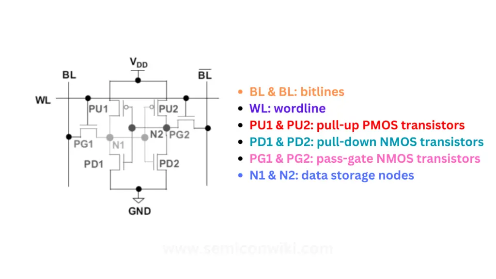
When diving into memory layout in 5nm technology, it’s helpful to understand how far we’ve come in SRAM design and the challenges that come with scaling. In this guide, I’ll walk you through some key concepts, focusing on SRAM layout and the evolution of FinFET technology that enables advanced nodes like 5nm.

Understanding the Basics of SRAM Layout
We’ve maintained the general structure of the 6T SRAM cell for decades, even as we’ve scaled down from planar transistors to FinFETs. You can think of SRAM as a highly optimized circuit, where every nanometer counts. Foundries push the boundaries of lithography to minimize the distances between contacts, isolation regions, and wires, often going beyond standard logic design rules.
Read also: What is Drain-Induced Barrier Lowering (DIBL)?
In earlier nodes like 65nm, you might notice imperfections in the gate patterns, such as rounded shapes, caused by optical limitations of 193nm photolithography. As we moved to smaller nodes, techniques like immersion lithography and multiple patterning helped extend the limits of photolithography. Today, in the 5nm era, extreme ultraviolet (EUV) lithography with a 13.5nm wavelength is important to continue scaling.
How FinFETs Revolutionized Memory Layout
The introduction of FinFETs at 22nm was a turning point for SRAM design. You probably know that FinFETs differ from planar transistors by offering a 3D structure, with the gate wrapping around the fin. This tri-gate design improves control over the channel, reduces short-channel effects, and enhances performance. For SRAM, FinFETs bring two main changes:
Quantized Electrical Width: Unlike planar transistors, where you can continuously size the width, FinFETs offer only discrete widths (multiples of the effective width. This quantization limits flexibility in transistor sizing.
Improved Integration Density: FinFETs boost current density, allowing fewer fins to achieve the same performance. In 5nm, the fin pitch is much smaller, and the layout becomes even denser.
Challenges in 5nm Memory Layout
Working on 5nm SRAM is exciting, but it comes with unique challenges. As you scale down:
Cell Area Shrinkage Slows: Although cell areas are smaller, the reduction rate has decelerated. For instance, high-density 6T cells have grown in normalized cell area as nodes shrink, reflecting increased lithography complexity.
Lithography Precision Matters: EUV lithography is a game-changer for 5nm, but it requires precise layout design to avoid errors during patterning. You’ll notice that even tiny deviations in fin or gate placement can impact performance.
Key Takeaways for Beginners
If you’re starting with 5nm memory layout, here are some tips:
- Master the Basics of FinFETs: Understand the quantized nature of electrical widths and how fin dimensions (width, height, and pitch) impact design choices.
- Focus on Foundry Rules: Foundries provide specialized design rules for SRAM at advanced nodes. Pay attention to minimum distances and patterning guidelines.
- EUV: The transition to EUV simplifies some aspects of patterning but requires careful alignment and adherence to tighter tolerances.
As you practice and experiment, you’ll see how 5nm technology brings both opportunities and constraints. By staying grounded in these fundamentals, you’ll be well-equipped to navigate the exciting world of advanced memory layout!