To prevent the Antenna Effect, we use several techniques. For example, we can route signals on higher metal layers, reduce the via area, or insert diodes to safely discharge any built-up charge. By applying these methods, we help protect the circuit and improve overall reliability. Let’s discuss the fixes for the Antenna Effect that we talked about in the previous post. Here are the common methods to address the antenna effect:
Read also: What is Antenna Effect?
Antenna Prevention Techniques
- Metal Hopping/Jog and Jump
- Dummy Transistor Insertion
- Antenna Diode Insertion
- Buffer Insertion
Metal Hopping/Jog and Jump
To mitigate the antenna effect, you can route the long net using two different metal layers. For instance, if a lengthy M2 wire is connecting to the gate, you can break the M2 layer and jump to a higher metal layer (e.g., M3) or any other available layer using vias. This approach reduces the accumulated charges on any single layer, preventing them from discharging through the gate oxide, since the M2 layer will have a smaller area. However, be aware that this might increase routing congestion.

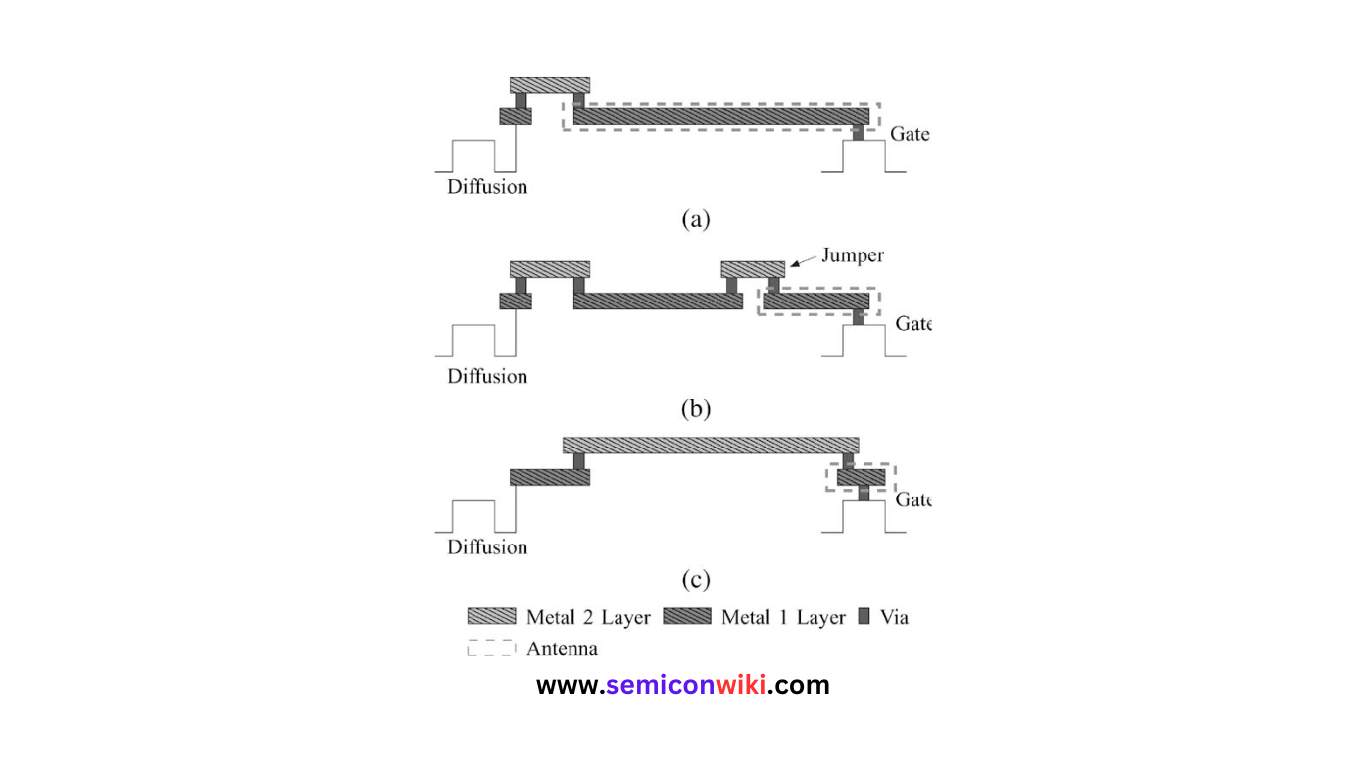
Why are top layers preferred over lower ones?
Fabrication starts from the lower metal layers and proceeds to the higher ones. By the time the higher metal layers are being fabricated, the interconnected lower layers are already completed. This makes it less likely for charges to accumulate excessively on the lower layers.
Read also: What is Electromigration Effect in VLSI?
Dummy Transistor Insertion
Inserting a dummy transistor increases the gate area, which reduces the antenna ratio. A lower antenna ratio helps to prevent antenna violations by distributing the charges over a larger area.
Read also: Top 10 Analog Layout Interview Questions(2024)
Antenna Diode Insertion
An antenna diode functions similarly to a reverse-biased diode. Inserting an antenna diode near the gate terminal can help discharge excessive charges. During the plasma etching process, which can occur at temperatures between 400 to 800 degrees Celsius (depending on the foundry), the diode can become thermally unstable and eventually enter a reverse saturation state, acting as a resistive path. This allows the accumulated charges to discharge through the diode, thereby protecting the gate.
Read also: How are guard rings used in IC layout to improve reliability and performance?
Buffer Insertion
Attaching a buffer to the net breaks it into smaller segments, which reduces the amount of charge that can accumulate in any single segment. This effectively mitigates the antenna effect by limiting the charge build-up.
By implementing these methods, you can effectively address and mitigate the antenna effect in your circuit designs. Each technique has its advantages and potential trade-offs, so choose the one that best fits your design constraints and goals.