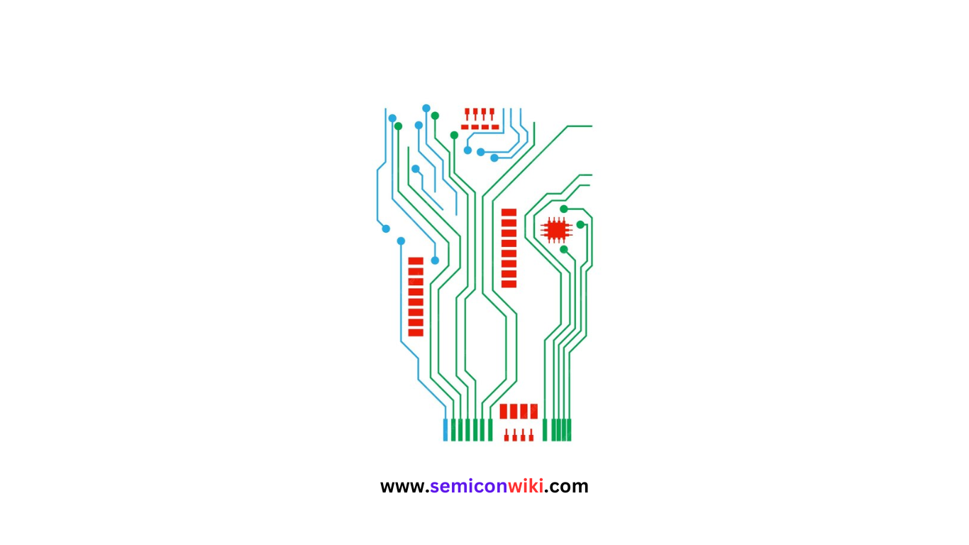
VLSI Design Questions with Answers (2025)
Very Large-scale integration (VLSI) is the process of integrating or embedding tens of thousands or more transistors on a single silicon semiconductor microchip. VLSI is a widely used technology in the design of microchip processors, components, and integrated circuits (IC). Because of this, most businesses are now converting to VLSI.
Leakage Current in CMOS: An In-Depth Analysis
Leakage current in CMOS circuits refers to the unwanted current that flows through the transistor even when it is turned off. This phenomenon occurs due to subthreshold leakage, gate oxide leakage, and junction leakage. Understanding and mitigating leakage current is essential for low-power design, especially in battery-operated and high-performance devices.
Comprehensive List of Sanity Checks in Physical Design
Sanity checks in physical design ensure the correctness and readiness of the design for tape-out. These checks include Design Rule Checks (DRC), Layout Versus Schematic (LVS) verification, Antenna Checks, Electrical Rule Checks (ERC), and Design for Manufacturability (DFM) guidelines. Each check validates different aspects of the design to avoid manufacturing issues.
https://pin.it/4jM5DszQd
Effective Low Power Design Techniques in Physical Design
Low power design techniques in physical design include clock gating, power gating, multi-threshold CMOS (MTCMOS), dynamic voltage and frequency scaling (DVFS), and the use of sleep transistors. These techniques reduce power consumption by minimizing dynamic and static power dissipation.
Read also: Latest Analog Layout Interview Questions (2024)
Module Constraint Types: Guide, Fence, and Region Explained
In physical design, module constraints like guides, fences, and regions help control the placement and routing of cells. A guide specifies preferred routing paths, a fence restricts cells to a specific area, and a region defines an area where certain cells must be placed. These constraints ensure efficient design layout and performance.
Understanding Process Corners in VLSI
Process corners in VLSI refer to the variations in semiconductor manufacturing processes that affect transistor speed and power. Common process corners include typical (TT), slow-slow (SS), fast-fast (FF), slow-fast (SF), and fast-slow (FS). Designers use these corners to simulate and ensure circuit performance under different conditions.
Exploring Process Variation in VLSI
Process variation in VLSI is the deviation in device parameters due to imperfections in the manufacturing process. These variations affect the performance, power consumption, and reliability of circuits. Understanding process variation is crucial for robust VLSI design and optimizing yield.
Key Reasons for Metastability in VLSI Designs
Metastability in VLSI designs occurs when a flip-flop or latch receives inputs that change near the clock edge, leading to unpredictable output states. This is typically caused by asynchronous signals, clock domain crossing, and insufficient setup and hold times. Addressing metastability is critical for reliable circuit operation.
Importance of Generated Clock and Virtual Clock in Design
Generated clocks are derived from primary clocks through clock dividers or multipliers, while virtual clocks are hypothetical clocks used for timing analysis. Generated clocks are essential for proper timing and synchronization, while virtual clocks help in defining timing constraints for complex designs without physically existing.
Identifying Sources of On-Chip Variation (OCV)
On-chip variation (OCV) arises from differences in manufacturing processes, voltage fluctuations, and temperature changes across a chip. OCV affects the timing and performance of circuits, making it essential to account for these variations during the design and verification phases.
The Phenomenon of Temperature Inversion on Lower Nodes
Temperature inversion occurs in advanced process nodes where the performance of transistors improves with increasing temperature. This counterintuitive behavior is due to the dominant impact of mobility degradation over velocity saturation at lower nodes, affecting timing analysis and thermal management strategies.
Types of Cells Used in Physical Design
Physical design uses various types of cells, including standard cells, decoupling capacitors (decaps), filler cells, antenna cells, and corner cells. Each cell type serves specific functions, such as logic implementation, mitigating antenna effects, and maintaining layout integrity.
Understanding Types of Variation in VLSI
Variations in VLSI include process variation, voltage variation, and temperature variation (PVT). Additionally, there are local variations like random dopant fluctuation and global variations like systematic lithography variations. Managing these variations is crucial for achieving reliable and predictable circuit performance.
Types of Violations in LVS and How to Address Them
LVS violations include mismatches between the layout and schematic, such as missing devices, incorrect connections, and parameter mismatches. Address these violations by cross-referencing the layout with the schematic, ensuring correct connectivity, and validating component parameters.
Understanding Clock Topologies in Digital Logic Chips: Tree, Mesh, and Hybrid Designs
Clock topologies in digital logic chips include tree, mesh, and hybrid designs. Clock trees offer simplicity and low power but may suffer from skew. Mesh topologies provide robustness and low skew but are power-intensive. Hybrid designs combine the benefits of both, optimizing performance and power consumption.
What Are Clock Gating and Power Gating?
Clock gating and power gating are techniques to reduce power consumption in digital circuits. Clock gating saves power by disabling the clock to inactive circuits, reducing dynamic power. Power gating cuts off the power supply to idle circuits, minimizing both dynamic and static power consumption.
What Are DRC and How Will You Fix Them?
Design Rule Checks (DRC) ensure that a design adheres to the manufacturing process’s geometric and electrical constraints. Fix DRC violations by modifying the layout to meet these constraints, such as adjusting spacing, width, and alignment of components and routing.
What Are Metal ECO and Base ECO?
Metal ECO (Engineering Change Order) involves changes limited to metal layers, allowing for late-stage design modifications without altering the base layers. Base ECO includes changes that affect both metal and base layers, often requiring more significant redesign efforts.
What Are Physical Design Inputs in Detail?
Inputs for physical design include the synthesized netlist, design constraints (SDC), technology files (LEF/DEF), cell libraries, power intent files (UPF/CPF), and floorplan information. These inputs guide the placement, routing, and optimization processes to create a manufacturable layout.
What Are the Advantages of Generating Clocks Internally?
Generating clocks internally reduces the need for external clock sources, minimizes clock distribution latency, and allows for dynamic clock adjustments. It enhances timing flexibility and can improve the overall performance and power efficiency of the design.
What Are the Inputs for Synthesis?
Inputs for synthesis include RTL code, design constraints (SDC), technology libraries, and configuration files. These inputs help the synthesis tool convert high-level design descriptions into an optimized gate-level netlist suitable for physical implementation.
What Are the Inputs of LVS?
Inputs for LVS include the layout netlist, schematic netlist, and corresponding rule files. These inputs allow the LVS tool to compare the layout against the schematic to ensure that they match and that the layout correctly implements the intended design.
What Are the Inputs of Physical Design?
Inputs for physical design encompass the synthesized netlist, design constraints (SDC), technology files (LEF/DEF), cell libraries, power intent files (UPF/CPF), and floorplan information. These inputs facilitate the placement, routing, and optimization of the chip layout.
What Are OCV and AOCV?
On-Chip Variation (OCV) accounts for variations within a single chip due to manufacturing imperfections. Advanced OCV (AOCV) further refines this by considering location-based and context-specific variations, providing more accurate timing analysis and improving design robustness.
What Are the Types of Physical Verification?
Physical verification types include Design Rule Checking (DRC), Layout Versus Schematic (LVS) verification, Electrical Rule Checking (ERC), Antenna Checks, and Design for Manufacturability (DFM) checks. These ensure the design adheres to manufacturing rules and operates correctly.
What Information is Presented in DEF?
The Design Exchange Format (DEF) file provides detailed information about the physical layout of the chip, including the placement of cells, routing of nets, blockages, and constraints. It is used for transferring design data between different EDA tools.
What is CMP (Chemical Mechanical Polishing)?
Chemical Mechanical Polishing (CMP) is a process used in semiconductor manufacturing to planarize the surface of the wafer. It combines chemical etching with mechanical polishing to achieve a smooth, flat surface, essential for subsequent photolithography steps.
What is Cross-Talk in VLSI?
Cross-talk refers to the unwanted interference between adjacent signal lines caused by capacitive coupling. It can lead to signal integrity issues, such as noise, delay, and data corruption. Mitigating cross-talk is crucial for reliable VLSI design.
What is Dynamic Power in CMOS Circuits?
Dynamic power is the power consumed by a CMOS circuit during switching activities. It is proportional to the capacitance, supply voltage, and switching frequency. Reducing dynamic power involves lowering voltage, minimizing capacitance, and optimizing switching activity.
What is Electromigration and How to Reduce It?
Electromigration is the gradual movement of metal atoms in interconnects due to high current densities, leading to eventual failure. Reducing electromigration involves using wider metal traces, lower current densities, and incorporating barrier layers to enhance reliability.
What Are HVT, LVT, and ULVT Cells?
HVT (High-Threshold Voltage), LVT (Low-Threshold Voltage), and ULVT (Ultra-Low-Threshold Voltage) cells are types of transistors used in CMOS design. HVT cells reduce leakage power, LVT cells offer higher speed, and ULVT cells balance speed and power efficiency.
What is Input and Output Delay?
Input delay is the time taken for an input signal to propagate through external circuitry before reaching a flip-flop or logic gate. Output delay is the time taken for a signal to propagate from a flip-flop or logic gate to external circuitry. Both are critical for accurate timing analysis.
What is Insertion Delay?
Insertion delay is the time taken for a clock signal to propagate from the clock source to a specific point in the clock network. It impacts the timing analysis and synchronization of flip-flops within a design.
What is Metal Fill Insertion?
Metal fill insertion involves adding non-functional metal shapes to a layout to achieve uniform metal density. This reduces dishing and erosion during CMP, ensuring better planarity and manufacturability.
What is Metal Slotting?
Metal slotting involves creating slots or holes in wide metal lines to reduce stress and prevent metal migration and cracking. It ensures mechanical reliability and reduces the impact of thermal expansion.
What is Temperature Inversion in Semiconductors?
Temperature inversion occurs when the performance of semiconductor devices improves with increasing temperature, contrary to typical behavior. It affects timing analysis and requires careful consideration in advanced process nodes for accurate design characterization.
What is the Clock Period and Levels of the Clock?
The clock period is the duration of one complete cycle of a clock signal, determining the operating frequency of the circuit. Clock levels refer to different stages of clock distribution, including the source, distribution network, and final endpoints.
What is the Content in .lib, .lef, and .tlef Files?
The .lib file contains standard cell library information, including timing, power, and functional data. The .lef file provides layout information such as cell dimensions and pin locations. The .tlef file is an extension of .lef, including additional technology-specific information.
What is the Difference Between ASIC and FPGA?
ASICs (Application-Specific Integrated Circuits) are custom-designed for specific applications, offering high performance and low power consumption. FPGAs (Field-Programmable Gate Arrays) are reconfigurable devices used for prototyping and versatile applications, providing flexibility at the cost of higher power and lower speed.
What is the Difference Between Crosstalk Delay and Crosstalk Noise?
Crosstalk delay refers to the timing delay caused by interference between adjacent signal lines. Crosstalk noise is the unwanted voltage induced on a signal line due to capacitive coupling from nearby switching lines, potentially causing logic errors.
What is the Dishing Effect in CMP?
The dishing effect in CMP is the excessive removal of material in wide metal areas, creating a concave surface. It affects planarity and can lead to non-uniform layer thickness, impacting subsequent manufacturing steps.
What is the Flow of Your VLSI Design Project?
The VLSI design project flow includes specification, RTL design, synthesis, floorplanning, placement, clock tree synthesis, routing, signoff verification (DRC/LVS), and tape-out. Each stage involves specific tools and methodologies to ensure a successful design.
What is the Impact of IR Drop on Cell Delay?
IR drop refers to the voltage drop in the power distribution network due to resistance. Significant IR drop can slow down the transistors, increasing cell delay and potentially causing timing violations in the circuit.
What is the Use of Placement Blockage?
Placement blockages restrict the placement of standard cells in specific areas, reserved for routing, power structures, or macro cells. This helps manage congestion and optimize the layout for better performance and manufacturability.
What is the Use of Shielding in VLSI Design?
Shielding involves placing grounded or power lines adjacent to signal lines to protect them from cross-talk and noise. It ensures signal integrity and reliable performance, especially in high-speed and sensitive circuits.
What is Useful Skew, Local Skew, and Global Skew?
Useful skew is the intentional adjustment of clock arrival times to meet timing requirements. Local skew refers to skew within a small group of flip-flops, while global skew considers the entire clock network. Managing skew is crucial for optimizing circuit performance.
What’s the Difference Between Design Rule Check (DRC) and Design for Manufacturability (DFM)?
DRC ensures the design adheres to geometric and electrical constraints for manufacturability. DFM goes beyond DRC, focusing on optimizing the design for yield, reliability, and manufacturability by considering additional factors like process variations and equipment capabilities.
Which Parameters Decide the Spacing Between Macros?
Parameters deciding the spacing between macros include routing congestion, thermal considerations, power distribution, and signal integrity. Adequate spacing ensures efficient routing, reduces cross-talk, and manages heat dissipation.
Why Do We Use Boundary Cells in Physical Design?
Boundary cells are used to ensure seamless connection and proper alignment between different regions or blocks in a design. They maintain signal integrity and prevent issues like signal reflection and cross-talk at the block boundaries.
Why Double Via Insertion is Important?
Double via insertion increases the reliability and robustness of interconnects by providing alternative current paths, reducing the risk of via failure. It enhances manufacturability and ensures better electrical performance under stress conditions.
Why is the Generated Clock Necessary in Physical Design?
Generated clocks are necessary for synchronizing various parts of the design that operate at different frequencies or phases. They help achieve precise timing control and improve the overall performance and functionality of the chip.
Why is Timing Analysis Important in Physical Design?
Timing analysis ensures that the design meets the required performance specifications by verifying that all signal paths meet their timing constraints. It prevents timing violations, ensuring reliable and predictable operation of the chip.