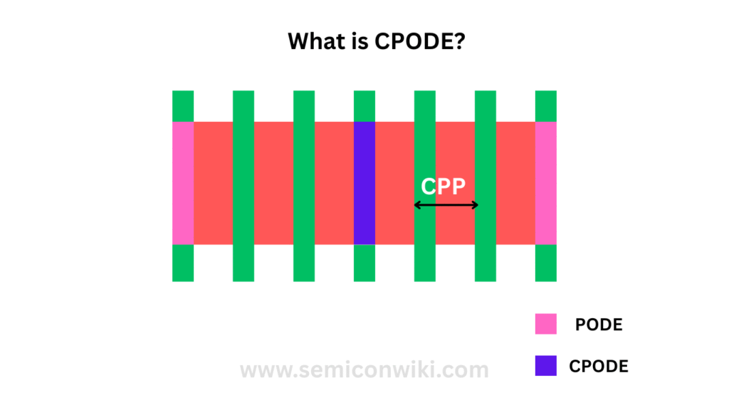
In VLSI layout, CPODE stands for Continuous Poly on Diffusion Edge. When you work with advanced nodes and multi-gate devices like FinFETs and GAA (Gate-All-Around) transistors, scaling becomes critical—especially in achieving tighter Contacted Poly Pitch (CPP). That’s where CPODE comes in.
When we talk about diffusion edges, we’re referring to the boundaries of active regions—those areas where actual transistor action happens (like source, drain, and gate formation). Now, when these regions sit close to each other, we need a clever way to isolate them while keeping the gate poly continuous for performance and density reasons. That’s exactly what CPODE does.
Read also: CoWoS Technology
CPODE stands for Continuous Poly on Diffusion Edge.
In the CPODE process, what we do is perform a dry etch at the active edge—essentially between two transistors—then fill that cut region with a dielectric like silicon nitride (SiN). This creates what’s called a fin-insulating structure, helping to separate neighboring transistors even if the poly runs continuously over both.
Why is this important to us as layout engineers? Because it allows us to scale down the pitch without compromising on isolation or risking shorts. However, it’s not without challenges. For example, if you’re not careful, source/drain contacts can bridge across that cut region during fabrication, causing shorts and hurting reliability. So, we always have to ensure our design and verification steps take this into account.
In short, when you use CPODE in VLSI layout, we’re enabling advanced scaling in a smart way—preserving both density and electrical isolation—which is essential for high-performance, low-power ICs at smaller nodes.
What is PODE?
When we design a standard cell using finFET technology, you and I often come across dummy polysilicon structures at the edges of the cell. These are known as PODE structures, or Polysilicon On Diffusion Edge. You don’t use them as real transistor gates, and I don’t connect them electrically in the design. Instead, we include them to protect the ends of the fins during manufacturing. These fins are delicate, and the PODE structures shield them from potential damage during fabrication steps.
While you might not use them for actual circuit functionality, the presence of PODE adds parasitic capacitance and resistance, which affects post-layout simulation accuracy. If we ignore PODE in our simulation models, the layout-versus-schematic (LVS) check might fail, because the physical layout (post-layout) contains these structures while the logical design (pre-layout) doesn’t.
Also, when we place standard cells next to each other, we can share PODE structures between adjacent cells to save space. This helps us pack the layout more densely. But in post-layout netlists, these shared PODEs look like functional transistors. So, we must ensure that we handle them correctly — for instance, by tying their gates to the substrate — so that no unintended behavior occurs.