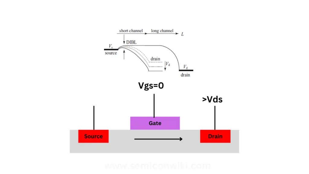
Drain-Induced Barrier Lowering (DIBL) is a phenomenon observed in short-channel MOS transistors. You can think of it as a reduction in the transistor’s threshold voltage caused by the interaction between the drain voltage and the channel’s potential barrier. Here’s how it works.

When you increase the drain-source voltage (VDSV_{DS}VDS) in a short-channel transistor, the electric field from the drain extends into the channel. This reduces the potential barrier at the source, making it easier for electrons to flow from the source to the drain. This effect lowers the threshold voltage, leading to an increase in subthreshold leakage current, even when the transistor is supposed to be “off.”
Read also: Why do We use Dummy Fill in the Layout Design?
DIBL becomes more significant as transistors shrink in size. In long-channel devices, the source and drain depletion regions are well-separated and have minimal interaction. However, in short-channel devices, the depletion regions from the source and drain overlap, amplifying DIBL.
Why does DIBL matter to you?
Power Consumption: DIBL increases subthreshold leakage current, which contributes to higher standby power in circuits, especially in deep-submicron technologies like 65nm or smaller.
Performance Impact: A lower threshold voltage affects the transistor’s switching characteristics and can lead to unwanted behavior in high-performance circuits.
Technology Scaling Challenge: As you work on advanced nodes like 7nm or 5nm, managing DIBL becomes critical in maintaining the balance between performance and power.
Understanding and mitigating DIBL is crucial, especially when designing for low-power applications or when dealing with high-density circuits. Techniques such as optimizing channel length, doping profiles, and device architectures (like FinFETs) help control DIBL effectively.
How to minimize DIBL (Drain-Induced Barrier Lowering)
Here’s how you can solve or minimize DIBL (Drain-Induced Barrier Lowering):
Increase Channel Length
Use transistors with slightly longer channel lengths to reduce the overlap of source and drain depletion regions.
Optimize Doping Profiles
Increase doping concentration in the channel to better control the electric field and reduce barrier lowering.
Use High-k Dielectric Materials
Replace traditional gate oxides with high-k materials to improve gate control and suppress DIBL.
Employ FinFET or Multi-Gate Transistors
Switch to advanced device structures like FinFETs or multi-gate transistors for better electrostatic control over the channel.
Reduce Drain Voltage (Vds)
Operate transistors at lower drain-source voltages to limit the effect of DIBL.
Body-Biasing Techniques
Apply a reverse bias to the substrate (or back gate) to increase the threshold voltage and suppress leakage currents.
By applying these techniques, you can effectively manage DIBL and maintain consistent transistor performance in advanced technology nodes.