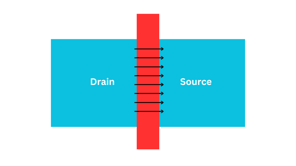
Parasitic Channel
A parasitic channel in a MOSFET happens when unintended conductive paths form between the source and drain regions due to poor design or environmental factors. You can think of these parasitic channels as unwanted MOSFETs, which cause leakage currents and hurt the device’s performance. They form outside the intended MOSFET area but in structures that resemble MOSFETs, like an n-p-n or p-n-p sequence of materials with a conductive gate separated by a dielectric.

Causes of Parasitic Channel Formation
- High Voltages: If you operate MOSFETs at high voltages, parasitic channels can form in the underlying silicon, especially if the dielectric (such as field oxide, FOX) isn’t thick enough.
- Low Doping: A lightly doped backgate increases the electric field effect, making it easier for a parasitic channel to form.
- Improper Metal Routing: If we route metal layers poorly, especially in active regions without FOX, these layers can act like parasitic gates and form unwanted channels.
Prevention Methods:
To avoid parasitic channels, you can apply several strategies:
Use Channel-Stop Implants: Before we apply field oxide (FOX) or shallow trench isolation (STI), channel-stop implants increase the doping in the substrate or well under the FOX. This raises the threshold voltage needed for parasitic channel formation, which is especially helpful in high-voltage environments.
Avoid Parasitic Gates in Sensitive Regions: You should minimize metal routing in active regions without field oxide to reduce the risk of parasitic channels. Use only the necessary lower metal layers to connect devices and avoid unnecessary interconnects.
Read also: What is Body (Back Gate) Effect?
Place Metal Routing on Higher Layers: By placing metal interconnects on higher layers, you increase the distance from the silicon, effectively thickening the dielectric. This makes it harder for parasitic channels to form.
Channel Stoppers: We can insert channel stoppers to locally increase the doping in the parasitic backgate region. This raises the threshold voltage and makes it more difficult for a parasitic channel to form.
Shield Parasitic Gates: Shielding techniques help by placing interconnect layers underneath potential parasitic gates, which blocks the formation of parasitic channels. This is particularly useful in high-voltage applications.
Enlarge the N-well: In PMOS devices, where parasitic p-channels might form between the PSD region and the p-substrate, enlarging the n-well can interrupt the parasitic channel.
Use Poly-Channel Stop Rings: In high-voltage designs, you can use poly-channel stop rings to prevent parasitic channels. These rings act as barriers by grounding or applying appropriate voltages to stop electric field buildup, preventing parasitic channel formation.
Conclusion:
Parasitic channels are an undesirable side effect in MOSFETs, especially at higher voltages. However, by applying the right techniques—such as using channel stoppers, optimizing metal routing, and applying shielding methods—you can effectively prevent parasitic channel formation and ensure reliable device performance.