


When you work on a VLSI layout, Gradient density DRC refers to the variation in pattern density across different regions of the chip. It shows how the density of metal, polysilicon, or other layers changes gradually across the layout. This concept is important because it directly affects the chip’s manufacturability and performance.
Why Should You Care About Gradient Density?
As we design chips, understanding gradient density becomes crucial for avoiding several issues:
- Planarization Issues: If the density isn’t uniform, the CMP (Chemical Mechanical Polishing) process might cause uneven surfaces or over-polishing in low-density regions.
- Stress Variation: When the density changes gradually, it can lead to mechanical stress, which impacts the performance and reliability of your devices.
- Etching Uniformity: Abrupt changes in density can make etching inconsistent, leading to deviations in feature sizes that affect the circuit’s functionality.
Gradient Density DRC (Design Rule Check) Example
Here two examples help you to understand this drc
Metal Density Gradient Violation
When we work on VLSI layouts, one critical issue we encounter is metal density gradient violations. If the metal density changes abruptly between two adjacent regions of the layout, it can cause planarization issues during the CMP (Chemical Mechanical Polishing) process, which we all know is crucial for achieving a flat wafer surface.

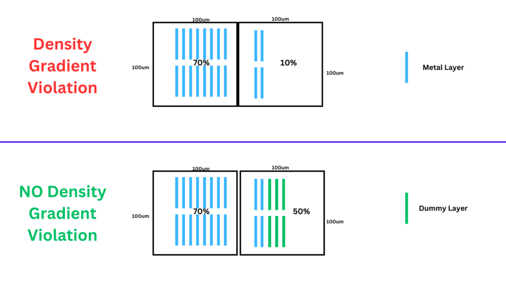
You should ensure that metal density does not vary by more than 50% across a 100μm x 1000μm window. For instance, if one region has 70% metal density and the adjacent region has 10%, this could trigger a gradient violation as shown in above figire, to solve this we should add a dummy fill in the empty region as shown in above figure.
Poly Density Gradient Violation
As you design your layouts, be mindful of polysilicon density gradient violations. Gradual or abrupt changes in polysilicon density across regions can lead to etching non-uniformity or stress effects, which directly impact transistor performance.
We must keep polysilicon density variation between adjacent regions below 10% across a 100μm x 100μm window. For example, if one region has 15% polysilicon density and the adjacent region has 28%, this would fail the DRC check.
How Do We Control Gradient Density?
Here’s how you and I can manage gradient density effectively:
- Dummy Fill: By adding dummy metal or polysilicon fills in low-density areas, we can balance the density across the layout.
- Density Rules: Foundries often give us specific density gradient rules to ensure smooth transitions between regions. Following these guidelines helps prevent problems.
- Automated Tools: We can use CAD tools to analyze and automatically adjust layouts to meet the required gradient density standards.
Conclusion
When you maintain acceptable gradient density, it helps us achieve better manufacturability, improved performance, and higher yield for the chip. Keeping these factors in mind makes your design not only more robust but also more production-friendly.
